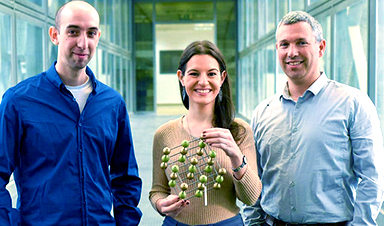
In recent years scientists have worked to create materials that can repair themselves, in order to deal with the swift degradation of devices we use at home. A discovery by Dr. Yehonadav Bekenstein and his team at the Technion could pave the way there.
One of the characteristics of living organisms is that they are capable of self-preservation. For example, when the skin is injured the body knows how to heal the wound by itself. One of the more exciting fields of research today is focusing on the attempt to reduce the gap between animate and inanimate. Groups of scientists and startups around the world are working to develop self-healing materials. Success in this effort is expected to spark a revolution in the realm of industrial manufacturing and could have major environmental ramifications.
Last week, a team from the Technion headed by Dr. Yehonadav Bekenstein, announced that it has developed semiconductor nanocrystals that can heal themselves. Their report was published in the journal of Advanced Functional Materials.
In today’s world, we have to replace our consumer electronics frequently, typically once every few years. The reason, in most cases, is reduced performance due to materials fatigue – a phenomenon that the manufacturers try to conceal. “They claim, for example, that their product is long-lasting and that the need to upgrade to newer products is to support newer software versions,” says Dr. Bekenstein.
But the malfunctioning of materials is unavoidable since every device suffers from degradation as a result of defects that accumulate during use over time. Aside from the frustration of having to go out to buy new devices every few years, the phenomenon also generates a heavy environmental footprint, since the recycling industry is struggling to handle the capacity of things we throw away.
“They still don’t know what to do with them, because the materials that are used in making the devices have already become defective,” says Bekenstein. “Of the items we throw away, 90 percent are sent to a landfill, even if we put them in recycling bins.” It’s no wonder, then, that manufacture of devices that can spontaneously repair their own defects is considered one of the most important goals in the world of materials engineering.
Prof. Dan Oron, a researcher in the Department of Molecular Chemistry and Materials Sciences at the Weizmann Institute of Science in Rehovot explains that, “every material used for making devices becomes damaged when it performs the operation for which it is used over time – the capacity of batteries declines, the transparency of the window lessens – all because of microscopic damage to the materials. How wonderful it would be if we could perform a simple process that would enable the material to repair itself, as is the case in biological systems. Solid materials for the most part cannot do that, but there are families of materials that are able to improve themselves through physical and chemical processes – whether due to an external stimulus or a spontaneous process. It never works perfectly, but it does slow the ageing of the materials.”
In recent years there has been progress in the field of developing soft materials that repair themselves; indeed, polymers that do that have already been produced. Perhaps we can expect that in the not-so-distant future it will be possible to manufacture clothes that patch themselves or renew their colors after many launderings.
Now scientists are hoping to devise a way to get semiconductors to repair themselves too. Despite their modest name, semiconductors are among the most important materials discoveries in the history of mankind. These are materials that neither conduct nor insulate electricity but can be altered in such a way that they can play both parts. They, therefore, serve as an infrastructure for virtually all of our modern electronic devices. The transmission or non-transmission of electricity are the basis for all digitization – zero or one. Silicon, for example, is a semiconductor, and the industry based on processing it to devices is flourishing”. “Semiconductors have changed the world because all the processors are made from them,” Bekenstein says. “The information revolution originates there – it all begins with an understanding of materials.”
The Technion’s new study was carried out by means of a family of semiconductors called halide perovskites. About five years ago researchers discovered that if a perovskite solar cell damaged due to use is left in the dark, under certain circumstances its operation returns to a level that’s almost identical to the way it functioned immediately after leaving the assembly line. This discovery led to the theory that these may be materials that can repair themselves.
Oron explains that halide perovskites are solid crystals, inside of which there is a constant movement of atoms that carry an electric charge (ions) – a characteristic not usually found in solid materials. “That’s the basis for the process of self-healing,” he says. “Defects are created in the crystal, but over time the ions find their way back and in that way the defects disappear.”
The process of repairing the crystal therefore takes place naturally, since it “wants” to rearrange itself into its initial, basic form, when the atoms inside the crystal are at their lowest energy state. In their new study, Bekenstein and doctoral students Sasha Khalfin and Noam Veber engineered nanoparticles of perovskites. In past studies, nanometric layers were created by abrading an ordinary-sized crystal, but the team discovered the right conditions under which a chemical reaction creates nucleation and the growth of nanocrystals. “We grew these crystals, which are on the verge of being the smallest crystals nature can create, in the lab, one to ten thousand of a human hair width” explains Bekenstein.
Nanocrystals are very convenient to use in research because an electron microscope dispatching a high-energy, focused beam can penetrate them and the transmitted electrons form an image, which is instructive when it comes to learning about the structure of the material. With large crystals that is impossible. The researchers sat for hundreds of hours in front of the electron microscope, trying to identify the processes that affect the structure of the crystal, in order to examine its self-healing abilities. “We observe the crystals day after day,” says Khalfin. “Once I sat for six straight hours.”
The team also filmed dozens of video clips and analyzed them with a computer, thus creating a picture of the dynamic that takes place in the nanocrystal. They discovered that the focused electron beam creates holes on the surface of the crystal, because the beam removes atoms from the material. After the holes are created, they migrate toward the center of the crystal. “We saw the holes being created and then pushed away from the edges, so that the margins always remained complete,” Bekenstein says.
As a result of this surprising observation, the researchers re-engineered the crystal. While during the first stage of the experiment they added organic molecules to the crystal while it was still growing, which attached onto its surface and stopped the growth so that it remained the size of a nanoparticle – during the second stage the team removed the organic layer on top in order to understand why the margins remained intact. Then Khalfin also identified an opposite phenomenon: Instead of the hole that was created moving to the center of the crystal, it seemed to be gradually pushed out to the sides, until in the end it was expelled from the crystal, which then returned to its original, whole state.
Bekenstein says that this marks the first-time scientists have been able to observe the healing process of a substance at the atomic level. “We managed to cause it, to understand what it comes from and then to control it, in other words, to understand what we have to put on the surface in order for it to happen,” he explains. “There are all kinds of defects that affect materials, and in this case, it was a most serious defect – a hole, in other words, part of the material was missing. We discovered that the perovskite crystal can return to its complete state if we rearrange things so the hole moves outward.”
This discovery constitutes an important step in understanding the mechanisms that enable perovskite nanoparticles to heal themselves, and is paving the way to the inclusion of such materials in electronic and solar devices. “We realized that the organic molecules are important when it comes to shaping the material, but they interrupt its process of self-repair,” Bekestein notes. “Now we can engineer devices that will exploit that situation.”
What is still unknown is the maximum distance to which a hole in a crystal can migrate and as a result, reach its edge and disappear from it. “In this case, it was a very short distance since we’re talking about a nanocrystal, but it’s not clear if that will happen with a big crystal. The science of self-healing has been understood, and now we have to engineer larger materials in which such a process will also take place,” he adds.
Perovskite materials have been known to science for over 100 years, but only in recent years has it become clear that lead-based halide perovskites have unique electro-optic characteristics. For his part, Prof. Oron says that this family of materials has been causing a revolution in solar cells in recent years. The solar cells now being used in rooftop panels are based on silicon, but about a decade ago scientists began to try to create solar cells from halide perovskites.
“At first the cells attained a level of efficiency of 4 percent and now it already reaches 25 percent,” says Oron. “On the other hand, standard silicon solar cells reach 23 percent efficiency in the laboratory and 16 to 18 percent in solar panels.” He says such rapid progress is “unprecedented in the world of solar cells.”
In addition to their great efficiency, the perovskite cells are created in a relatively simple process from a solution, in contrast to silicon cells, which are crystallized at high temperatures in a process that requires a great deal of energy. Oron says that it takes three years of activity on the part of a silicon solar cell, to restore the energy that was invested in creating it in the first place, and therefore the perovskite cells are “an opening to a revolution in the creation of cheap and simple cells [for use in solar panels].”
The professor does note that the use of perovskite cells can be problematic; for instance, they contain lead and perovskite materials that dissolve in water. Therefore, their use is limited at present. “But in terms of technology, it’s a breakthrough. Many startups are involved in it.”
Oron says that a few years ago, a research group headed by Prof. David Cahen at the Weizmann Institute damaged a relatively large perovskite crystal with a laser beam, and then kept track of the process whereby the damage was repaired. “In the most recent study, Bekenstein did the same thing, but created the damage with an electron microscope, which enabled him to actually see both the damage and the dynamic of the repair. That made it possible to see the movement of atoms inside the crystal itself, which opened a new window to understanding the self-healing processes,” says Oron.
Oron says that he believes that the day will come when perovskites will become part of the leading technology used to produce solar cells and perhaps electronics and electro-optics as well.
The Technion researchers point to two additional advantages of the perovskite materials they have developed. As opposed to materials from the previous generation, the new perovskites do not contain toxic lead and should be recyclable.
“Today it’s hard to recycle used electronic devices, because the material itself is damaged over time,” Bekenstein notes. “Due to our invention we’ll be able to recycle material so that it will assume its complete shape, the same as on the day it was manufactured, and then reuse it.” These materials may be of great importance in places where it is impossible to replace defective materials – for example, in the solar panels that help to power satellites in space.
Bekenstein cites a story in Tractate Ta’anit in the Talmud about Abba Hilkiah, the grandson of Honi the Circle Maker, whom the sages sent for so that he would pray for rain. He went with the emissaries and arrived at a field of thorns. The rabbi lifted his robe. The others asked why he did that, and Hilkiah said: “Wounds in the body can be healed, but the tears in clothing can’t be mended.”
“Maybe that’s about to change,” smiles Bekenstein. “In effect, what man wants is for his creations to resemble those of God. The ancient Greeks already tried to achieve that by means of the statues they created, but even if those works looked like living creatures, they couldn’t repair or heal themselves as God’s creations could. We’re a long way from that, but within nanoparticles, we have been able to imitate the self-repair of material.”
News
Molecular Manufacturing: The Future of Nanomedicine – New book from NanoappsMedical Inc.
This book explores the revolutionary potential of atomically precise manufacturing technologies to transform global healthcare, as well as practically every other sector across society. This forward-thinking volume examines how envisaged Factory@Home systems might enable the cost-effective [...]
Ancient bacteria strain discovered in ice cave is resistant to some modern antibiotics
In the depths of Scarisoara cave in Romania sits one of the world’s biggest underground glaciers, a monumental slab of ice the size of roughly 40 Olympic swimming pools that began to form around [...]
Scientists Identify “Good” Bacteria That May Prevent Long COVID
According to the WHO, about 6% of people worldwide who get COVID-19, roughly 400 million people, later develop a long-lasting form of the illness. That shows the condition remains a significant public health challenge. In [...]
New book from Nanoappsmedical Inc. – Global Health Care Equivalency
A new book by Frank Boehm, NanoappsMedical Inc. Founder. This groundbreaking volume explores the vision of a Global Health Care Equivalency (GHCE) system powered by artificial intelligence and quantum computing technologies, operating on secure [...]
RNA Recycling Extends Lifespan
Summary: Researchers discovered a biological “trash disposal” mechanism that directly controls how fast we age. While circular RNA has long been known to accumulate in cells as we get older, this study proves for the [...]
Cancer’s Deadly Paradox: How Tumors Break Their Own DNA To Keep Growing
Cancer’s strongest gene switches push DNA into damaging overdrive, creating repeated breaks and repairs that may fuel tumor evolution while exposing possible therapeutic weak spots. A new study indicates that cancer can harm its own genetic [...]
NanoMedical Brain/Cloud Interface – Explorations and Implications. A new book from Frank Boehm
New book from Frank Boehm, NanoappsMedical Inc Founder: This book explores the future hypothetical possibility that the cerebral cortex of the human brain might be seamlessly, safely, and securely connected with the Cloud via [...]
Our books now available worldwide!
Online Sellers other than Amazon, Routledge, and IOPP Indigo Global Health Care Equivalency in the Age of Nanotechnology, Nanomedicine and Artifcial Intelligence Global Health Care Equivalency In The Age Of Nanotechnology, Nanomedicine And Artificial [...]
Ryugu asteroid samples contain all DNA and RNA building blocks, bolstering origin-of-life theories
All the essential ingredients to make the DNA and RNA underpinning life on Earth have been discovered in samples collected from the asteroid Ryugu, scientists said Monday. The discovery comes after these building blocks [...]
Is Berberine Really a “Natural Ozempic”?
Often labeled a “natural Ozempic,” berberine is widely discussed as a metabolic aid. Yet research suggests its influence may lie deeper. In recent years, berberine has gained significant attention as a supposed “natural way” [...]
Viagra Ingredient Shows Promise for Rare Childhood Brain Disease in Surprising Study
A rare childhood disease with no approved treatment may have an unexpected new therapeutic candidate. Sildenafil, the active ingredient also sold under the brand name Viagra, may help reduce symptoms in people with Leigh [...]
In a first for China, Neuracle’s implantable brain-computer interface wins approval
In a landmark development, Neuracle Medical Technology has secured the country’s first-ever approval for an implantable brain-computer interface (BCI) system designed to restore hand motor function in patients with spinal cord injuries, in a [...]
A Cambridge Lab Mistake Reveals a Powerful New Way to Modify Drug Molecules
A surprising lab discovery reveals a light-powered way to tweak complex drugs faster, cleaner, and later in development. Researchers at the University of Cambridge have created a new technique for altering complex drug molecules [...]
New book from NanoappsMedical Inc – Molecular Manufacturing: The Future of Nanomedicine
This book explores the revolutionary potential of atomically precise manufacturing technologies to transform global healthcare, as well as practically every other sector across society. This forward-thinking volume examines how envisaged Factory@Home systems might enable the cost-effective [...]
Scientists Discover Simple Saliva Test That Reveals Hidden Diabetes Risk
Researchers have identified a potential new way to assess metabolic health using saliva instead of blood. High insulin levels in the blood, known as hyperinsulinemia, can reveal metabolic problems long before obvious symptoms appear. It is [...]
One Nasal Spray Could Protect Against COVID, Flu, Pneumonia, and More
A single nasal spray vaccine may one day protect against viruses, pneumonia, and even allergies. For decades, scientists have dreamed of creating a universal vaccine capable of protecting against many different pathogens. The idea [...]
